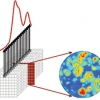
This article looks at the advantages of synchrotron radiation for infrared microspectroscopy, selected applications and its future potential.
Spectroscopy Articles
Pages
E.A.H. Timmermans and J.J.A.M. van der Mullen*
Department of Applied Physics, Eindhoven University of Technology, PO Box 513, 5600 MB Eindhoven, The Netherlands. E-mail address [email protected]
G.J. Price, G.W. Fraser, J.F. Pearson, I.B. Hutchinson, A.D. Holland, J. Nussey, D. Vernon, D. Pullan and K. Turner
Space Research Centre, Department of Physics and Astronomy, University of Leicester, Leicester LE1 7RH, UK. E-mail: [email protected]
David Chenery and Hannah Bowring
Smith & Nephew Group Research Centre, York Science Park, Heslington, York YO10 5DF, UK
T. Wirtz and H.-N. Migeon
Laboratoire d’Analyse des Matériaux, Centre de Recherche Public - Gabriel Lippmann, 162A, av. de la Faïencerie, L-1511 Luxembourg, [email protected]
Introduction
Glow Discharge Mass Spectrometry (GDMS) is one of the most powerful solid state analytical methods for the direct determination of traces, impurities and depth profiling of solids.1–5 Glow discharge mass spectrometers, which are commercially available with fast and sensitive electrical ion detection, allow direct trace elemental determination in solid materials with good sensitivity and precision in the concentration range lower than ng g–1.6
Luisa Mannina,a,b Anatoli P. Sobolevb and Annalaura Segreb
aUniversity of Molise, Faculty of Agriculture, 86100 Campobasso, Italy
bInstitute of Chemical Methodologies, CNR, 00016 Monterotondo Staz., Rome, Italy
Moore’s law* dictates microelectronics researchers to make integrated circuit (IC) devices smaller and to put them as close to each other as possible on a chip. This results in a better performance and a larger functionality of the chips. However, these devices also require a good electrical isolation from each other. This is in general done by the formation of a thick local oxide in the “field region” between the devices. In 1970, researchers from Philips1 invented the so-called LOCOS (LOCal Oxidation of Silicon) technique to achieve this isolation. Using a Si3N4 mask, the silicon is thermally oxidised in the nitride-free field regions. Figure 1 (left) shows a typical LOCOS structure. Although LOCOS seemed a perfect solution at that time, it came with a lot of problems, many of them related to mechanical stresses. Thermal oxidation of Si to SiO2 occurs together with a 125% volume expansion. As a result, the oxide grown in the field region, called the “field oxide,” exerts large forces on the surrounding silicon. Another major drawback of this technique is the so-called “bird’s beak,” caused by the lateral growth of the oxide under the nitride mask. This bird’s beak not only affects the intended device length, it also introduces large local mechanical stresses in the silicon, because of volume expansion, and it also deforms the nitride film. These stresses often resulted in the generation of dislocations in the silicon, which are quite harmful for the devices.
Alan Street
Technical Director, Oxford Instruments Superconductivity
S.Y. Luk,a N. Patela and M.C. Daviesb
aMolecular Profiles Ltd, 1 Faraday Building, Nottingham Science & Technology Park, University Boulevard, Nottingham NG7 2QP, UK. E-mail: [email protected]
bLaboratory of Biophysics and Surface Analysis, School of Pharmaceutical Sciences, University of Nottingham, Nottingham NG7 2RD, UK
Dipl. Chem. FH Ch. Schanzer and Prof. Dr H.G. Bührer
Department of Chemistry, Zurich University of Applied Sciences Winterthur (ZHW), CH-8401 Winterthur, Switzerland
S.E.J. Bell,a* E.S.O. Bourguignon,a A. O’Grady,a J. Villaumiea and A.C. Dennisb
aSchool of Chemistry, The Queen’s University of Belfast, Belfast, BT9 5AG, Northern Ireland, UK
bAvalon Instruments Ltd, 10 Malone Road, Belfast BT9 5BN, Northern Ireland, UK
J. Sabine Becker
Central Department of Analytical Chemistry, Research Centre Jülich, D-52425 Jülich, Germany
Luis Oliveira and Manuel Pais Clemente
CETO – Centro de Ciências e Tecnologias Ópticas, Rua Caldas Xavier, Nº38, 6º E, 4150 Porto, Portugal. E-mail: [email protected]
The study of the mineralogical phases of archaeological ceramics may be very helpful in unravelling the history of an ancient sherd, particularly by means that investigate the process of its production. Micro-Raman spectroscopy offers advantages as a non-destructive, or even better, a non-sampling technique.
It is now more than fifty years ago that Felix Bloch and Edward Mills Purcell independently discovered a phenomenon called nuclear magnetic resonance (NMR). Only a few years later, in 1952, both received the Nobel Laureate Physics award for this discovery. Purcell and Bloch were the first to “listen” to the whisperings of hydrogen. They eventually obtained an NMR spectrum representing the different “pitches” of the nuclei, a property, which reflects the physico–chemical (electronic) neighbourhood of the nucleus.
Chemical imaging spectroscopy is an exciting new analytical advance that answers commonly asked questions such as what chemical species are in a sample, how much of each is present, and most importantly, where are they located? Through the fusion of traditional infrared spectroscopy with powerful microscopic and macroscopic imaging capabilities, chemical imaging spectroscopy answers all these questions simultaneously, in a single rapid measurement.
This article discusses the development of new Certified Reference Materials (CRMs) for use in determining the essential accuracy and linearity of the Transmission scale of a conventional UV/vis spectrophotometer.
Ever since the development of inductively coupled plasma-mass spectrometry in the mid 1980s, there have been certain applications or specific analyses that have been regarded as difficult or impossible to address using the technique. This article explores the optimisation of the technique in high matrix samples.


