Kálmán Vad,a Attila Csika and Gábor A. Langerb
aInstitute of Nuclear Research, Hungarian Academy of Sciences, H-4001 Debrecen, PO Box 51, Hungary. E-mail: [email protected]; web: http://www.atomki.hu/SNMS
bDepartment of Solid State Physics, University of Debrecen, H-4010 Debrecen, PO Box 2, Hungary
Introduction
The decrease of dimensions and increasing complexity of thin-film and multilayer structures require the application of methods that provide information down to the nanometre scale. The quantification of nanostructures and surface layers with high sensitivity is often of crucial importance in monitoring product quality. Sensitive elemental analysis, together with a quantitative chemical analysis, is a prerequisite for the preparation of thin-layer structures of good quality. Several methods based on ion sputtering exist for this purpose, e.g. secondary ion mass spectrometry (SIMS), X-ray photoelectron spectroscopy (XPS), Auger electron spectroscopy (AES) and secondary neutral mass spectrometry (SNMS). While in XPS and AES the surface is analysed by various forms of electron spectroscopy after sputtering, in SIMS and SNMS the sputtered particles themselves are detected by a mass spectrometer. This results in a difference in their practical applications. Electron spectroscopy is capable of giving information about the material structure and the chemical state of elements. The SIMS and SNMS techniques yield information about the elemental composition and the depth profile of elements.
The purpose of this article is to give a comparative description of two methods applying ion-beam sputtering in materials research: secondary ion and neutral mass spectrometries (SIMS and SNMS). We shall illustrate the application of the latter by reports on a compositional analysis of perovskite oxides and on an investigation of nanoscaled multilayer structures.
Ion-beam sputtering
Ion-beam sputtering is a widely used method for surface modification in nanoscience and nanotechnology. During sputtering, the sample surface is bombarded by a low- or medium-energy ion beam. The primary ions of the beam suffer ion–atom collisions at the surface and induce atom–atom collisions in the target. As a result of an atomic collision cascade, the primary ions are backscattered from the target or stopped in it. If some target atoms near the surface acquire high enough energy from the kinetic energy of primary ions to overcome the surface binding energy, they are emitted in the form of either secondary ions or neutral atoms. The emitted secondary ions, being in a negatively or positively charged state, are analysed by SIMS, the emitted secondary neutral atoms and molecules are analysed by SNMS. Most of the sputtered particles are neutral in charge (atoms, atomic clusters, molecules); only a small portion (~1%) consists of positively or negatively charged ions. Since the emitted particles originate predominantly from the uppermost one or two monolayers, SIMS and SNMS are destructive methods which characterise the surface. The primary ions are generally those of an inert gas (e.g. neon, argon, krypton), a reactive gas (oxygen), metal (Ga, Cs) or of C60 molecules. The ion energy can range from a few hundred eV up to 20 keV.1
The detailed analysis of the emitted particles provides information about the lateral and depth distribution of the sample composition. While the yield of the secondary ions emitted in the sputtering process can be significantly affected by the chemical composition of the sample surface, which is known as the matrix effect, the yield of secondary neutral particles (atoms and molecules) is independent of the matrix effect. The matrix effect causes some difficulties in the evaluation of Auger-electron, photoelectron and secondary ion yields; it strongly influences the quantitative analytical methods used for characterising a sample. To eliminate the errors of the matrix effect, one must calibrate the methods.
Secondary neutral mass spectrometry
SNMS is one of the most efficient methods to determine the depth distribution of atomic compositions.2 In SNMS the processes of emission and ionisation of sputtered particles are strictly separated, which is the main difference between SNMS and SIMS. The sample surface is bombarded by an ion beam and the sputtered neutral particles, atoms and atomic clusters are detected by a mass spectrometer after some post-ionisation, which can be performed by an electron beam, electron gas or laser beam. Of these, the most efficient way to ionise the emitted neutral particles is laser beam ionisation. The laser-ionised fraction of the neutrals can be as high as 10% in contrast to 1% in the case of electron gas ionisation. As the ionisation takes place at the moment when the neutral particles leave the surface, the ionisation probabilities of different elements are almost identical. Therefore, the matrix effect burdening SIMS does not exist in SNMS signals which are directly correlated with the actual concentrations in the sample via a particle-specific but matrix-independent detection factor.3
The results described below were achieved on an INA-X type SNMS system produced by SPECS GmbH Berlin. This system uses low-pressure radio frequency plasma (Electron Cyclotron Wave Resonance plasma) for both sputter and post-ionisation. The sample surface is bombarded with the ions extracted from the plasma (Direct Bombardment Mode) by applying high frequency voltage between the sample and aperture (High Frequency Mode) to enable charge compensation. The bombarding ion energy ranges from 100 eV up to 2 kV. The sample temperature can be continuously varied from 100 K up to 900 K. The residual gas ions are suppressed by energy dispersive ion optics. The detection system is a quadrupole mass spectrometer operating in the 1–340 amu range, supplemented with a secondary electron multiplier. The maximum analysable area is 14 mm in diameter. Due to the highly uniform sputtering current density over the entire analysed area and the low primary ion energy (a few hundred eV), a depth resolution of 1 nm can be achieved. An example for this resolution and the schematic arrangement of SNMS are shown in Figure 1. A Co/Ru multilayer sample with 3.6 nm double-layer thickness was prepared by magnetron sputtering in order to study its magnetic properties. Minimal matrix effect and the absence of preferential sputtering allowed us to perform a very accurate material analysis of the structure. It must be stressed, however, that SNMS is suitable for measuring the chemical composition of almost any type of sample, because the flux of atoms sputtered from the sample is representative of the stoichiometry of the uppermost layer for the case of homogeneous materials. Surface roughness up to 1 µm scale is tolerated by this method. In the case of insulators the applicability of SNMS is achieved using the high frequency mode to eliminate charge accumulation on the sample surface. Otherwise the study of insulators can cause serious problems in surface analysis methods, where electron emission or excitation is applied.
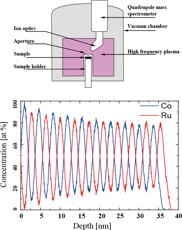
Figure 1. Upper: Schematic drawing of an SNMS instrument. Lower: Depth profile analysis of a Co/Ru thin film multilayer structure by SNMS. The double-layer thickness is 3.6 nm.
In the following part of this article we discuss two examples of the applicability of the SNMS technique in determining the chemical composition of perovskite oxides and in an investigation of electrodeposited alloy layers.
Experimental results
Composition determination of doped perovskites
Doped perovskites have become a highlight of modern solid state physics due to the discovery of high-temperature superconductivity (HTS) and colossal magnetoresistance (CMR). Some types of perovskites (cuprates) show superconductivity, others (manganates, cobaltates) show CMR. The common feature of these two families of compounds is that their electromagnetic properties depend sensitively on oxygen content. The superconducting transition temperature of Bi2Sr2Ca(Pr)Cu2O8 + δ cuprates or the magnetic and electronic transport properties of La(Sr)Co(Fe)O3 – δ perovskites change dramatically with δ, the deviation from the nominal oxygen content. Apart from doping, the oxygen deficiency is influenced by the particulars of the preparation process, such as calcination and sintering. Simultaneous determination of constituents is of crucial importance for an adequate sample characterisation. The demand for analytical techniques for accurate determination of the elemental concentration of perovskite oxides increases with the development of the experimental technique. SNMS is a successful technique for the analysis of perovskites and for studying their doping processes. In Figure 2 we demonstrate the efficiency of SNMS in chemical analysis, even of very tiny samples, by measuring the mass spectrum of a Bi2Sr2Ca0.86Pr0.14Cu2O8.4 sample. The most exciting challenge in this measurement was the small sample mass. The lateral dimensions of the sample were a few hundred µm, the thickness was a few µm, so the mass was only 3 µg. A picture of the sample is shown in the inset of Figure 2. The inner circular surface was sputtered with Ar ions extracted from the plasma. In the determination of the oxygen content of the sample not only was the oxygen peak taken into account, but also the oxide peaks, because oxygen can leave the perovskite oxides during sputtering in the form of molecular clusters. Here the broad mass range of our SNMS setup was an asset. The chemical concentration of doped cobaltites La1 – xSrxCo0.975Fe0.025O3 – δ was determined similarly. From these measurements it turned out that the oxygen content depends sensitively on the doping level of Sr.
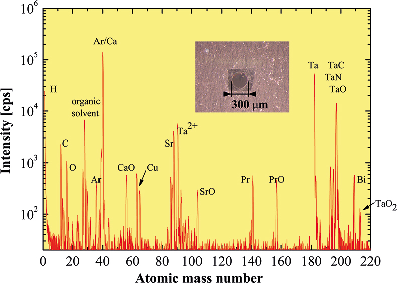
Figure 2. Mass spectrum of a Bi2Sr2Ca0.86Pr0.14Cu2O8.4 high transition temperature superconducting sample. The inset shows the small sample which was investigated.
Analysis of electrodeposited structures
Electrodeposition of alloys has long been a focus of research from both technical and scientific viewpoints. In traditional large-scale applications of electrodeposition, the coating produced is thick enough to neglect all transient effects at the start of the deposition. Recently, the application of electrodeposition for producing nanometre thick multilayer structures4 raised new questions. The changes of the structure of the deposit over the total deposit thickness, which is often much below the micrometre range, has become of interest. Furthermore, down to the nanometre scale, the initial transient effect needs to be well understood.
Research of such types of electrodeposited magnetic materials is required by the microelectronic industry. Fe–Co–Ni alloys are at the forefront of research because higher saturation magnetisation and lower coercivity are achieved with the ternary alloys than with the binary ones. Due to its flexibility and low cost, electrodeposition of high magnetic moment materials is a viable alternative among the production methods.
We have performed conventional depth profile analysis (i.e. starting the analysis from the final deposit surface) and reverse depth profile analysis (i.e. detaching the multilayers from the substrate and starting the analysis from the substrate side) of electrodeposited Fe–Co–Ni alloys by SNMS.5 We have found that the reverse sputtering method gave a much better depth resolution at the vicinity of the substrate. The reverse SNMS spectra showed that the deposition of Fe–Co–Ni alloys starts with the formation of an iron-rich zone, followed by an increase in Co concentration, then the nickel content increases and a steady-state alloy composition is achieved at a film thickness higher than 500 nm. It was also found that if a high current density is applied in the deposition, the initial depth pattern reproduces itself twice before the composition becomes stable. We have concluded that the varying depth profile is a consequence of the anomalous nature of the co-deposition of the alloy components, the depletion of the electrolyte with respect to the metal salts, and the dependence of the intensity of the hydrogen evolution on the deposit surface composition. Figure 3 shows the result of a depth profile analysis of a Fe–Co–Ni alloy.
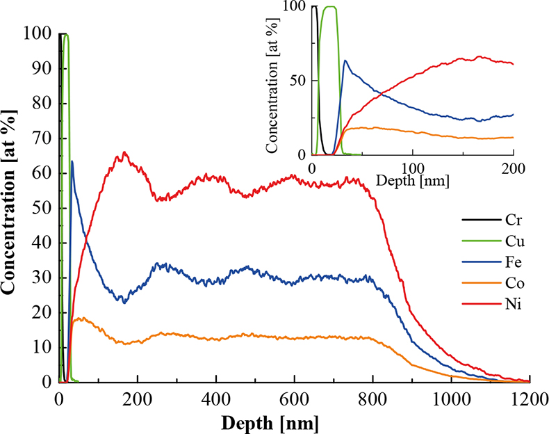
Figure 3. Reverse depth profile of a Fe–Co–Ni sample deposited at 24 mA cm–2 current density. The 5 nm Cr and 20 nm thick Cu layers were sputtered onto the surface of a Si substrate prior to the electrodeposition process.
Summary
In this article we briefly described the mechanism of ion sputtering and secondary neutral mass spectrometry. Through examples we demonstrated the applicability of the SNMS method for the quantitative composition analysis of perovskite samples and for the depth profile analysis of multilayers and electrodeposited alloy systems. The lack of matrix effect together with high depth resolution is the main advantage of SNMS over other methods based on ion sputtering.
Acknowledgements
The authors wish to express many thanks to L. Forró (EPFL, Lausanne) and L. Péter (SZFKI, Budapest) for preparing the HTS and electrodeposited samples.
References
- K. Wittmaack, in Practical Surface Analysis, Ed by D. Briggs and M.P. Seah. John Wiley & Sons, Chichester and New York, p.105 (1992).
- H. Oechsner and L. Reichert, Phys. Lett. 23, 90 (1966). https://doi.org/10.1016/0031-9163(66)90273-3; R. Jede, O. Ganschow and U. Kaiser, in Practical Surface Analysis, Ed by D. Briggs and M.P. Seah. John Wiley & Sons, Chichester and New York, p. 425 (1992).
- Wucher, F. Nowak and W. Reuter, J. Vac. Sci. Technol. A 6, 2265 (1988). https://doi.org/10.1116/1.575022.
- G.L. Katona, Z. Berényi, L. Péter and K. Vad, Vacuum 82, 270 (2008). https://doi.org/10.1016/j.vacuum.2007.07.035.
- Csik, K. Vad, E. Tóth-Kádár and L. Péter, Electrochem. Comm. 11, 1289 (2009). https://doi.org/10.1016/j.elecom.2009.04.027.